Model Answer:
India envisions becoming a global semiconductor hub to ensure strategic digital autonomy and capture a share of the $500 billion global market, transitioning from import-dependence to indigenous manufacturing.
1. Challenges Faced by the Semiconductor Industry in India
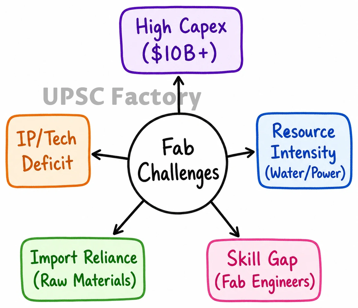
- High Capital Outlay: Fabs require massive upfront investment (often $10B+) and endure 4–5 year gestation periods.
- Resource Intensity: Manufacturing demands uninterrupted, high-capacity power and millions of gallons of ultra-pure water daily.
- Technological Complexity: India currently lacks indigenous Intellectual Property (IP) and R&D maturity in advanced node engineering.
- Raw Material Dependency: Over-reliance on imports for critical inputs like neon gas, rare earth elements, and specialized chemicals.
- Skilled Talent Deficit: Acute shortage of specialized fabrication and metallurgical engineers, despite a strong VLSI design workforce.
- Fierce Global Competition: Competing against established, highly subsidized global ecosystems (US CHIPS Act, Taiwan, South Korea).
- Ancillary Ecosystem Void: Absence of a robust domestic supply chain for specialized equipment delays end-to-end production.
2. Salient Features of the India Semiconductor Mission (ISM)
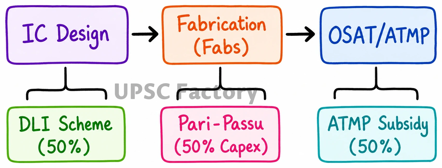
- Massive Financial Outlay: Dedicated ₹76,000 crore ($10B) comprehensive package to catalyze the ecosystem.
- Pari-Passu Fiscal Support: Flat 50% financial support of project cost for setting up Semiconductor and Display Fabs.
- OSAT/ATMP Incentives: 50% capital expenditure support for Assembly, Testing, Marking, and Packaging facilities (Micron’s ATMP facility, Sanand).
- Design Linked Incentive (DLI): Financial incentives up to 50% of eligible expenditure for domestic semiconductor design and IP creation.
- Node-Agnostic Approach: Pragmatic support spanning mature nodes (28nm+) crucial for automotive/telecom sectors (Tata-PSMC Dholera Fab).
- Autonomous Nodal Agency: ISM operates as an independent division under Digital India Corporation to appraise and negotiate proposals.
- SCL Modernization: Focused upgradation of the Semi-Conductor Laboratory (SCL), Mohali, for advanced R&D and commercial prototyping.
By aggressively bridging infrastructure deficits and leveraging ISM’s targeted incentives, India can successfully pivot from a passive chip consumer to a resilient node in the global semiconductor value chain.